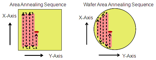
Overview
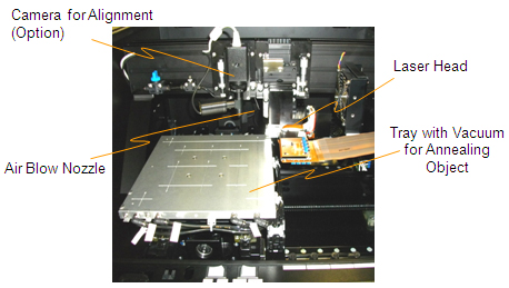
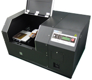
Inside of the Tool
This tool can be used not only for anneal process but also Punching, Cutting process for various materials such as organic and inorganic thin film and wafer etc.
<Example1>
Crystallization on Phase-change Material
(Ge-Sb-Te)
(POL-A3)
<Example2>
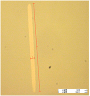
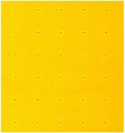
Punching of Thin Film Silicon (POL-A1)
Hole Size: 18um
Interval: X,Y,Z direction200μm
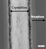
<Example3>
Crystallization of Thin Film Silicon
(POL-A1)
| Model | POL-A1 | POL-A3 | |
|---|---|---|---|
| Laser Head |
Wavelength, Max Laser Output |
405 +/-5nm, 360mW | 810 +/-10nm, 2600mW |
| Spot Size of Long Axis |
Approx. 18um | Approx. 30, 50, 100, 200um | |
| Spot Size of Short Axis |
Approx. 0.5um | Approx. 1um | |
| Maximum Object Size | 8inch wafer, 200 x 200mm Substrate | ||
| X-Y Stage | Stage Motor | Stepping Motor | |
| Max Scan Speed | 10 - 500mm/s | ||
| X-Axis Resolution | 2um | ||
| Y-Axis Resolution | 1um | ||
| Connect for External Output | RS232C (For setting an annealing conditions) | ||
| Power Consumption | 700VA | ||
| Air Supply | 0.2 - 0.6MPa (For fixing the object on the tray) | ||
| Dimensions (W x H x D) | Approx. 900 x 500 x 600mm | ||
| Weight | Approx. 94kg | ||